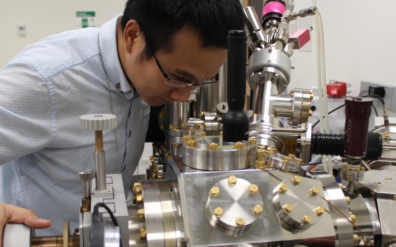
LEEM measurements
- Field of view: 2 mm - 150 mm
- Spatial resolution: atomic resolution in Z direction, 10 nm in XY directions
- Energy of probe electrons: 0-500 eV
- XY motion of sample: ± 5 mm
- Sample heating during imaging: up to 2,000 K
- Sample cooling during imaging: ~ 150 K with LN2
- Gas exposure during imaging: pO2 ~ 1×10⁻⁵ Torr
In-situ MBE synthesis
- Electron beam evaporator (suitable for metal, semiconductor and insulator source materials ; can reach temperature up to 3,500℃)
The source material can be replaced without venting the main chamber
- Knudsen-cell thermal evaporation source
Sample cleaning
- Sputtering with Argon ion (energy: 0-500 eV / 1,000 eV / 1,500 eV / 2,000 eV ; current 0-10 µA
- Annealing: up to 2,000 K, PID temperature control
Click here to download our LEEM data
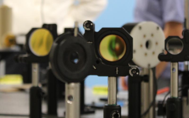
The variable-temperature scanning near-field optical microscope (SNOM)
- Current setup and capabilities of the VT-SNOM:
- Determination of the complex dielectric function of
materials with a spatial resolution of ~ 20 nm
- Quartz tuning fork’based detection (W and Au etched tips, afm tapping oscillation 20 – 60 kHz)
- Working temperature range: 10 K - 300 K
- Energy: currently optimized for mid-IR & 0.1 - 1 THz
Add Bruker 66 – operating from far IR to UV range, currently optimized for mid-infrared operation